
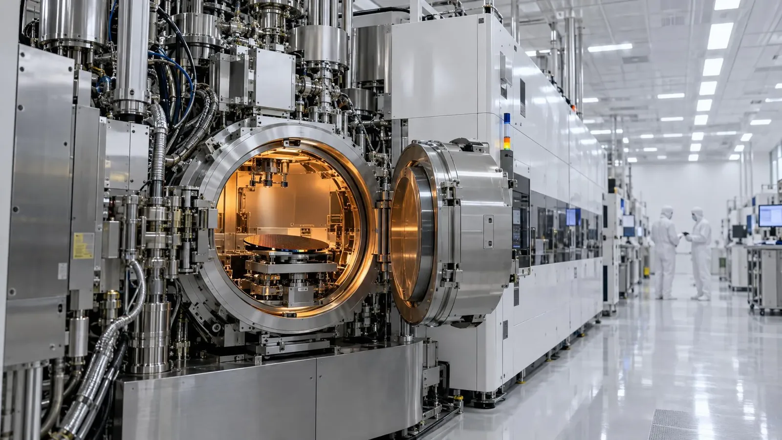
Applied Materials unveiled its Equipment and Process Innovation and Commercialization Center in Sunnyvale, California, on October 12, 2026, presenting it as a $5 billion capital investment and the largest facility for collaborative semiconductor process and equipment research. The 600,000-square-foot building contains nearly four acres of advanced cleanroom space for joint work on technologies three to four generations ahead of production. The move matters for AI business because chip complexity tied to AI infrastructure now requires faster transfer of materials research into volume manufacturing.
How EPIC replaces sequential chip development
Capital spending is expected to scale over time to approximately $5 billion as customer projects commence, according to a footnote to the investment figure. The unveiling day began with a summit hosted by Dr. Prabu Raja, president of the Semiconductor Products Group, where research leaders from design, manufacturing and equipment companies discussed industry challenges. President and CEO Gary Dickerson said scaling AI infrastructure drives new complexity across the chipmaking roadmap and requires a re-engineered model of collaboration. The company expects additional firms and organizations to join the ecosystem over time.
The center is designed to remove handoffs between three separate environments used for decades: foundational materials research, equipment and process development, and process integration with pilot production. Under the new model, specialists who invent materials, build equipment and manufacture chips work in one facility in parallel rather than in sequence. Partners work alongside Applied scientists and engineers in secure learning cycles, each bringing its own roadmap challenges and engineering teams. Raja said EPIC is the only place where materials, process technology and equipment will be innovated in parallel, which increases the success rate of new materials.
Applied expects returns on both sides of the partnerships from this operating model. Chipmakers gain earliest access to next-generation materials and equipment, shorter learning cycles and a faster path to volume production. Applied itself gains visibility across several generations of emerging technology challenges, which informs where it directs research investments. The building required more than six million construction hours, with foundations holding enough concrete to fill 34 Olympic-sized swimming pools. Its steel structure holds enough steel to build two Eiffel Towers, while 34 roof trusses cover the cleanrooms, each spanning nearly 300 feet and weighing as much as 12 school buses.
What the new R&D model means for AI hardware
For companies that buy or deploy AI compute, the practical effect is a shorter distance between laboratory materials and factory-ready process equipment. If parallel development works as described, accelerators, memory and advanced packaging for energy-efficient AI architectures could reach high-volume manufacturing faster. That matters most for large buyers planning data center capacity around next-generation nodes, where equipment availability sets procurement timelines. Smaller firms do not buy process tools directly, but they feel the result through earlier supply and broader choice of chips and systems.
The model still carries conditions that buyers and partners should verify before drawing conclusions. Joint work happens in secure learning cycles, so access to results will depend on partnership terms rather than open availability. The sustainability description cites an all-electric central volatile organic compound abatement unit, electrified central facilities and a design to recycle about 40 percent of water, yet operating performance will only be clear after customer projects commence. The announcement by itself does not guarantee shorter cycle times or specific product dates, so questions about project selection, intellectual property and capacity allocation remain central.
The marker to watch is which customer projects start inside EPIC and how quickly they move toward pilot production. Statements from TSMC on work beyond the 2-nanometer node, Intel on more than a trillion transistors in a package by 2030, and Micron, Samsung Electronics and SK hynix on memory and packaging point to the first test cases. If those collaborations produce equipment and process options adopted for volume manufacturing, the parallel approach will have proven its commercial value.